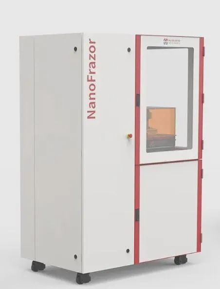
2025/05/21 Wed. 9:00 am-11:00 am
Meeting Room, Fourth Floor, TICNN, Tianjin University
Title 1: Unlocking Novel Nanofabrication with NanoFrazor Patterning and Processing Technology-From Andrea Ubezio
Title 2: NanoFrazor Lithography for advanced 2D&3D nanodevices
From Dr ZhengMing Wu

<01>
Unlocking Novel Nanofabrication with NanoFrazor Patterning and Processing Technology-From Andrea Ubezio
Abstract
How is nanolithography possible with the NanoFrazor? How is the lithography pattern later transferred to your substrate?
During the talk, I will explain the most important features of the NanoFrazor software and the most common pattern transfer techniques, trying to answer these two questions.
We will see critical software functionalities such as the Closed Loop Lithography (CLL), Mix & Match, Automated Overlay, Stitching and Smart Field Splitting, with short videos capturing the tool in live action, highlighting the importance of the features for your applications.
We will explore the most common NanoFrazor process flows with examples of applications, to understand how the lithography step can be integrated with metallization and etching with resolution below 20 nm, and grayscale structuring with resolution below 1 nm.
Speaker Biography
Andrea studied Materials Engineering (BSc, MSc) and Nanotechnology at Politecnico of Milano (Italy), then completed a MPhil research program in the Electronic and Computer Engineering Department at the Hong Kong University of Science and Technology (China). His research focus was semiconductor and perovskite nanowire arrays for novel optoelectronic devices. He is now a Research & Development Engineer at Heidelberg Instruments Nano. His main tasks involve technical customer support and training, research of high-resolution processing techniques and NanoFrazor tool development.
<02>
Title 2: NanoFrazor Lithography for advanced 2D&3D nanodevices
From Dr ZhengMing Wu
Abstract
“Thermal scanning probe lithography (t-SPL) using the NanoFrazor from Heidelberg Instruments enables simultaneous patterning and inspection of nanoscale structures. Along with its integrated direct laser writer, this technology allows mix & match lithography of nanodevices. Combined with markerless second layer alignment and automation features, this versatile tool solves complex fabrication challenges and enables applications in various fields including nanophotonics, quantum nanoelectronics, nanobiosystems, and emerging materials research.
Short CV
ZhengMing Wu received her PhD in University of Basel, she fabricated nano-devices using UV and e-beam lithography in the group of Prof Schoenberger. In 2009, she joined Nanosurf and successfully set up and developed the sales network in Asia. In 2014, she joined Heidelberg Instruments Nano as the first salesperson and established a worldwide sales network. ZhengMing can be found at international conferences, seminars, and workshops where she explains the NanoFrazor technology and discusses applications.

